ADCMP601
FEATURES
Rail-to-Rail, Very Fast, 2.5 V to 5.5 V, Single-Supply TTL/CMOS parators ADCMP600/ADCMP601/ADCMP602
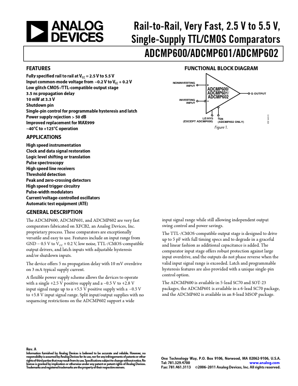
FUNCTIONAL BLOCK DIAGRAM
NONINVERTING INPUT
10 m V sensitivity rail to rail at VCC = 2.5 V Input mon-mode voltage from
- 0.2 V to VCC + 0.2 V Low glitch CMOS-/TTL-patible output stage 3 ns propagation delay 15 m W at 3.3 V Shutdown pin Single-pin control for programmable hysteresis and latch Power supply rejection > 60 d B Improved replacement for MAX999
- 40°C to +125°C operation
INVERTING INPUT
ADCMP600/ ADCMP601/ ADCMP602
Q OUTPUT
LE/HYS (Except ADCMP600)
SDN (ADCMP602 Only)
Figure 1.
APPLICATIONS
High speed instrumentation Clock and data signal restoration Logic level shifting or translation Pulse spectroscopy High speed line receivers Threshold detection Peak and zero-crossing detectors High speed trigger circuitry Pulse-width modulators Current-/voltage-controlled oscillators Automatic test equipment (ATE)
GENERAL DESCRIPTION
The ADCMP600, ADCMP601, and ADCMP602 are...