Datasheet Details
| Part number | ADCLK907 |
|---|---|
| Manufacturer | Analog Devices |
| File Size | 1.23 MB |
| Description | (ADCLK905 - ADCLK925) Ultrafast ECL Clock / Data Buffers |
| Datasheet |
 ADCLK907 Datasheet ADCLK907 Datasheet
|
|
|
Download the ADCLK907 datasheet PDF. This datasheet also covers the ADCLK925 variant, as both devices belong to the same (adclk905 - adclk925) ultrafast ecl clock / data buffers family and are provided as variant models within a single manufacturer datasheet.
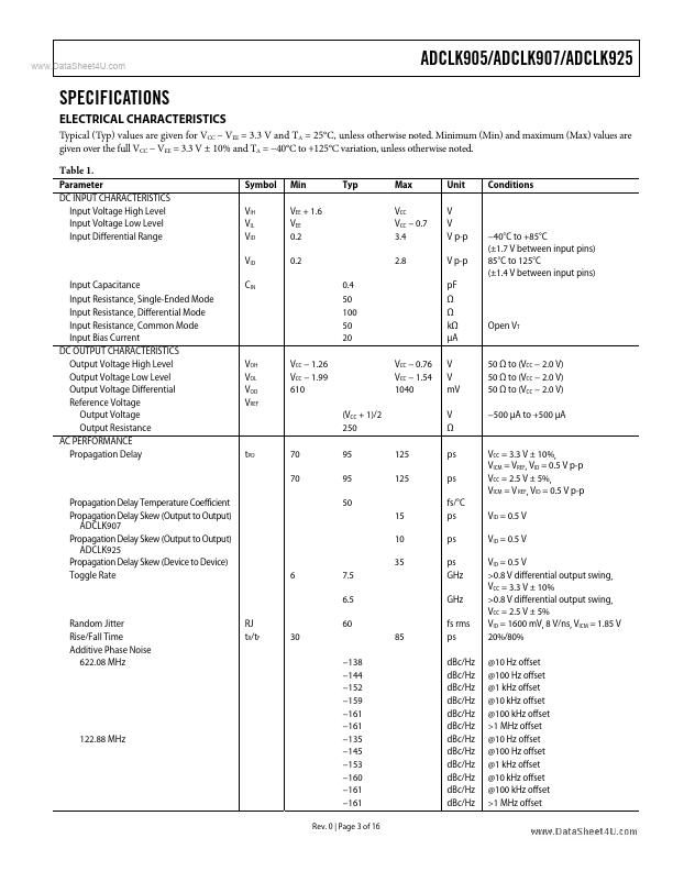
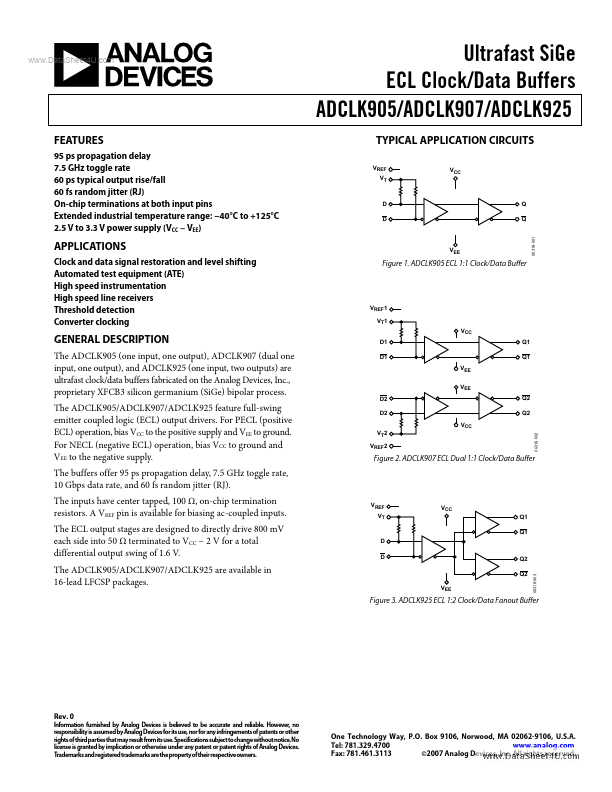
The ADCLK905 (one input, one output), ADCLK907 (dual one input, one output), and ADCLK925 (one input, two outputs) are ultrafast clock/data buffers fabricated on the Analog Devices, Inc., proprietary XFCB3 silicon germanium (SiGe) bipolar process.
| Part number | ADCLK907 |
|---|---|
| Manufacturer | Analog Devices |
| File Size | 1.23 MB |
| Description | (ADCLK905 - ADCLK925) Ultrafast ECL Clock / Data Buffers |
| Datasheet |
ADCLK907 Datasheet
|
|
|
|
| Part Number | Description | Manufacturer |
|---|---|---|
| ADC-0802 | A/D Converters | Harris |
| ADC-0803 | A/D Converters | Harris |
| ADC-0804 | A/D Converters | Intersil Corporation |
| ADC-0804 | A/D Converters | Harris |
| ADC-10-4+ | Directional Coupler | Mini-Circuits |
| Part Number | Description |
|---|---|
| ADCLK905 | (ADCLK905 - ADCLK925) Ultrafast ECL Clock / Data Buffers |
| ADCLK914 | Open-Collector HVDS Clock/Data Buffer |
| ADCLK925 | (ADCLK905 - ADCLK925) Ultrafast ECL Clock / Data Buffers |
| ADCLK944 | SIGE CLOCK FANOUT BUFFER |
| ADCLK946 | SiGe Clock Fanout Buffer |
The following content is an automatically extracted verbatim text from the original manufacturer datasheet and is provided for reference purposes only.