ADA4510-2 Overview
Description
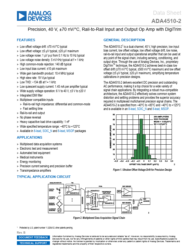
The ADA4510-21 is a dual-channel, 40 V, high precision, low input bias current, low offset voltage, low offset voltage drift, low noise, rail-to-rail input and output operational amplifier that can be used at any point of the signal chain, including sensing, conditioning, and output drive. Through the use of Analog Devices, Inc., proprietary DigiTrim™ technique, the ADA4510-2 achieves best-in-class low offset drift (±70 nV/°C typical, ±500 nV/°C maximum) and low offset voltage (±5 μV typical, ±20 μV maximum), simplifying temperature calibrations in precision designs.
Key Features
- Low offset voltage drift: ±70 nV/°C typical
- Low offset voltage: ±5 μV typical, ±20 μV maximum
- Low voltage noise: 1 μV p-p from 0.1 Hz to 10 Hz typical
- Low voltage noise density: 5 nV/√Hz typical at f = 1 kHz
- High common-mode rejection: 140 dB typical
- Low input bias current: ±10 pA maximum
- Wide gain bandwidth product: 10.4 MHz typical
- High slew rate: 19 V/μs typical
- Low THD: -134 dB at f = 1 kHz
- Low quiescent supply current: 1.45 mA per amplifier typical