AD9695
AD9695 is Dual Analog-to-Digital Converter manufactured by Analog Devices.
Data Sheet
14-Bit, 1300 MSPS/625 MSPS, JESD204B, Dual Analog-to-Digital Converter AD9695
Features
JESD204B (Subclass 1) coded serial digital outputs Lane rates up to 16 Gbps
1.6 W total power at 1300 MSPS 800 m W per ADC channel
SNR = 65.6 d BFS at 172 MHz (1.59 V p-p input range) SFDR = 78 d BFS at 172.3 MHz (1.59 V p-p input range) Noise density
- 153.9 d BFS/Hz (1.59 V p-p input range)
- 155.6 d BFS/Hz (2.04 V p-p input range) 0.95 V, 1.8 V, and 2.5 V supply operation No missing codes Internal ADC voltage reference Flexible input range 1.36 V p-p to 2.04 V p-p (1.59 V p-p typical) 2 GHz usable analog input full power bandwidth >95 d B channel isolation/crosstalk Amplitude detect bits for efficient AGC implementation 2 integrated digital downconverters per ADC channel 48-bit NCO Programmable decimation rates Differential clock input SPI control Integer clock divide by 2 and divide by 4 Flexible JESD204B lane configurations On-chip dithering to improve small signal linearity
APPLICATIONS munications Diversity multiband, multimode digital receivers
3G/4G, TD-SCDMA, WCDMA, GSM, LTE General-purpose software radios Ultrawideband satellite receiver Instrumentation
Oscilloscopes Spectrum analyzers Network analyzers Integrated RF test solutions Radars Electronic support measures, electronic counter measures, and electronic counter-counter measures High speed data acquisition systems DOCSIS 3.0 CMTS upstream receive paths Hybrid fiber coaxial digital reverse path receivers Wideband digital predistortion
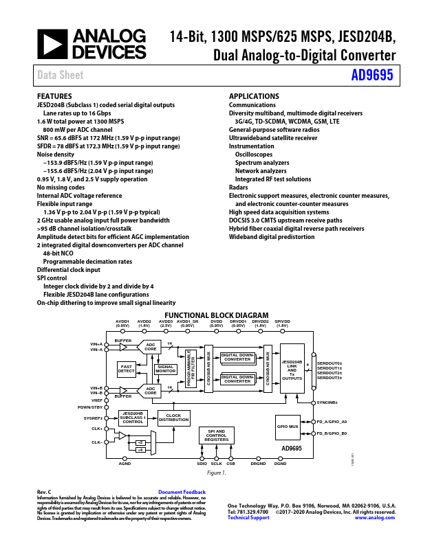
AVDD1 (0.95V)
AVDD2 (1.8V)
FUNCTIONAL BLOCK DIAGRAM
AVDD3 AVDD1_SR (2.5V) (0.95V)
DVDD DRVDD1 DRVDD2 SPIVDD
(0.95V) (0.95V) (1.8V)
(1.8V)
PROGRAMMABLE FIR FILTER
CROSSBAR MUX CROSSBAR MUX
15660-001
VIN+A VIN- A
BUFFER
CORE
FAST DETECT
SIGNAL MONITOR
VIN+B VIN- B VREF PDWN/STBY
SYSREF±
CLK+
CLK-...