AD9525
Overview
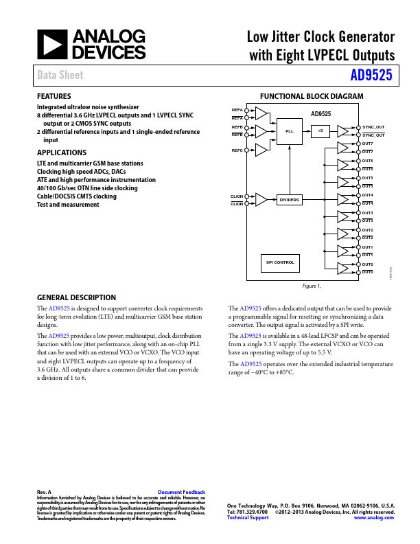
The AD9525 is designed to support converter clock requirements for long-term evolution (LTE) and multicarrier GSM base station designs. The AD9525 provides a low power, multioutput, clock distribution function with low jitter performance, along with an on-chip PLL that can be used with an external VCO or VCXO.