AD7610
AD7610 is Unipolar/Bipolar Programmable Input PulSAR ADC manufactured by Analog Devices.
FEATURES
Multiple pins/software programmable input ranges: 5 V, 10 V, ±5 V, ±10 V Pins or serial SPI®-patible input ranges/mode selection Throughput: 250 k SPS 16-bit resolution with no missing codes INL: ±0.75 LSB typ, ±1.5 LSB max (±23 ppm of FSR) SNR: 94 d B @ 2 k Hz i CMOS® process technology 5 V internal reference: typical drift 3 ppm/°C; On-chip temperature sensor No pipeline delay (SAR architecture) Parallel (16- or 8-bit bus) and serial 5 V/3.3 V interface SPI-/QSPI™-/MICROWIRE™-/DSP-patible Power dissipation 90 m W @ 250 k SPS 10 m W @ 1 k SPS 48-lead LQFP and LFCSP (7 mm × 7 mm) packages
AGND AVDD PDREF PDBUF IN+ IN- SWITCHED CAP DAC REF
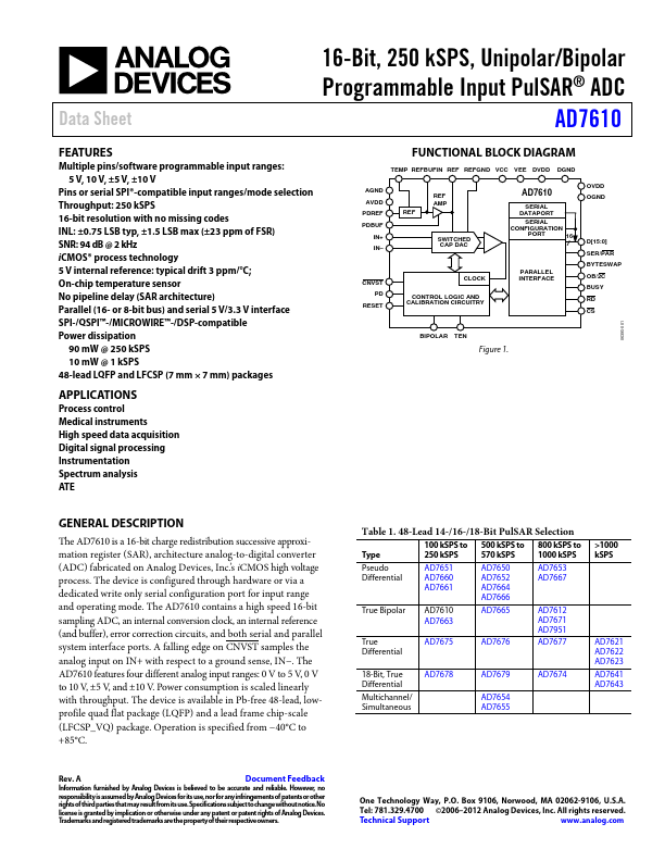
FUNCTIONAL BLOCK DIAGRAM
TEMP REFBUFIN REF REFGND VCC VEE DVDD DGND OVDD OGND
REF AMP
SERIAL DATAPORT SERIAL CONFIGURATION PORT 16
D[15:0] SER/PAR BYTESWAP
CNVST PD RESET
CLOCK CONTROL LOGIC AND CALIBRATION CIRCUITRY
PARALLEL INTERFACE
OB/2C BUSY RD CS
06395-001
BIPOLAR
Figure 1.
APPLICATIONS
Process control Medical instruments High speed data acquisition Digital signal processing Instrumentation Spectrum analysis ATE
GENERAL DESCRIPTION
The AD7610 is a 16-bit charge redistribution successive approximation register (SAR), architecture analog-to-digital converter (ADC) fabricated on Analog Devices, Inc.’s i CMOS high voltage process. The device is configured through hardware or via a dedicated write only serial configuration port for input range and operating mode. The AD7610 contains a high speed 16-bit sampling ADC, an internal conversion clock, an internal reference (and buffer), error correction circuits, and both serial and parallel system interface ports. A falling edge on CNVST samples the analog input on IN+ with respect to a ground sense, IN- . The AD7610 features four different analog input ranges: 0 V to 5 V, 0 V to 10 V, ±5 V, and ±10 V. Power consumption is scaled linearly with throughput. The device is available in Pb-free 48-lead, lowprofile quad flat package (LQFP) and a lead frame chip-scale...