AD5143
AD5143 is Nonvolatile Digital Potentiometer manufactured by Analog Devices.
- Part of the AD5123 comparator family.
- Part of the AD5123 comparator family.
FEATURES
10 kΩ and 100 kΩ resistance options Resistor tolerance: 8% maximum Wiper current: ±6 m A Low temperature coefficient: 35 ppm/°C Wide bandwidth: 3 MHz Fast start-up time < 75 μs Linear gain setting mode Single- and dual-supply operation Wide operating temperature:
- 40°C to +125°C 3 mm × 3 mm package
APPLICATIONS
Portable electronics level adjustment LCD panel brightness and contrast controls Programmable filters, delays, and time constants Programmable power supplies
GENERAL DESCRIPTION
The AD5123/AD5143 potentiometers provide a nonvolatile solution for 128-/256-position adjustment applications, offering guaranteed low resistor tolerance errors of ±8% and up to ±6 m A current density in the Ax, Bx, and Wx pins.
The low resistor tolerance and low nominal temperature coefficient simplify open-loop applications as well as applications requiring tolerance matching.
The linear gain setting mode allows independent programming of the resistance between the digital potentiometer terminals, through the RAW and RWB string resistors, allowing very accurate resistor matching.
The high bandwidth and low total harmonic distortion (THD) ensure optimal performance for ac signals, making the devices suitable for filter design.
The low wiper resistance of only 40 Ω at the ends of the resistor array allows for pin to pin connection.
The wiper values can be set through an I2C-patible digital interface that also reads back the wiper register and EEPROM contents.
The AD5123/AD5143 are available in a pact, 16-lead, 3 mm × 3 mm LFCSP. The devices are guaranteed to operate over the extended industrial temperature range of
- 40°C to +125°C.
SCL SDA ADDR
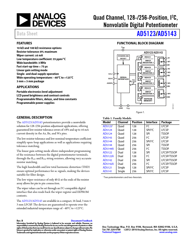
FUNCTIONAL BLOCK DIAGRAM
POWER-ON RESET
AD5123/AD5143
RDAC1
INPUT REGISTER 1
SERIAL INTERFACE 7/8
RDAC2
INPUT REGISTER 2
RDAC3
INPUT REGISTER 3
RDAC4
INPUT REGISTER 4
EEPROM MEMORY
A1 W1 B1 A2 W2 B2
W3 B3
W4 B4
10878-001
GND VSS
Figure 1.
Table 1. Family Models
Model Channel Position
AD51231 Quad
AD5124...