AOP610
Description
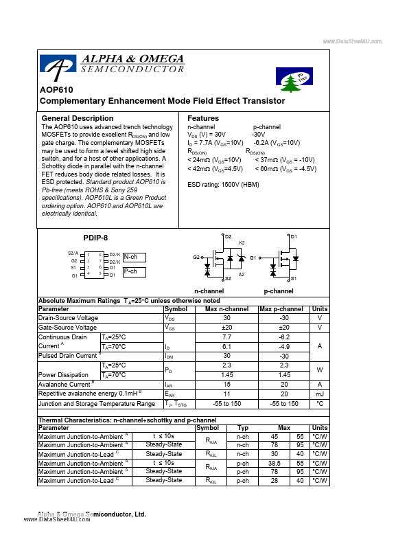
The AOP610 uses advanced trench technology MOSFETs to provide excellent RDS(ON) and low gate charge.
Key Features
- Copper, in a still air environment with TA=25°C
- The value in any given application depends on the user's specific board design
- The current rating is based on the t≤ 10s