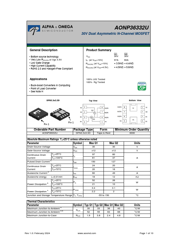
Datasheet4U Logo Datasheet4U.com

AONP36332U Datasheet 30V Dual Asymmetric N-Channel MOSFET

Manufacturer: Alpha & Omega Semiconductors

Overview: AONP36332U 30V Dual Asymmetric N-Channel MOSFET General.

General Description

• Bottom source technology • Very Low RDS(ON) at Vgs 4.5V • Low Gate Charge • High Current Capability • RoHS 2.0 and Halogen-Free Compliant Product Summary VDS ID (at VGS=10V) RDS(ON) (at VGS=10V) RDS(ON) (at VGS=4.5V) Q1 Q2 30V 30V 97A 60A < 3.5mΩ < 4.4mΩ < 4.5mΩ < 5.6mΩ Applications • Buck-boost Converters in Computing • Point of Load Converter • See Note H DFN3.3x3.3D 100% UIS Tested 100% Rg Tested Top View Bottom View Q2 Q1 Pin 1 Pin 1 Orderable Part Number AONP36332U Package Type Form DFN3.3x3.3D Tape & Reel Minimum Order Quantity 3000 Absolute Maximum Ratings TA=25°C unless otherwise noted Parameter Symbol Max Q1 Max Q2 Drain-Source Voltage VDS 30 30 Gate-Source Voltage VGS ±12 ±12 Continuous Drain Current TC=25°C TC=100°C ID 97 61 60 37 Pulsed Drain Current C IDM 150 127 Continuous Drain Current TA=25°C TA=70°C IDSM 24 20 20 16 Avalanche Current C IAS 60 49 Avalanche energy L=0.01mH EAS 18 12 TC=25°C Power Dissipation B TC=100°C PD 52 21 26 10 TA=25°C Power Dissipation A TA=70°C PDSM 3.4 2.2 3.1 2 Junction and Storage Temperature Range TJ, TSTG -55 to 150 Units V V A A A mJ W W °C Thermal Characteristics Parameter Maximum Junction-to-Ambient A Maximum Junction-to-Ambient A D Maximum Junction-to-Case Symbol RqJA RqJC Typ Q1 Typ Q2 Max Q1 Max Q2 30 33 36 40 52 55 63 66 1.9 3.8 2.4 4.8 Units °C/W °C/W °C/W Rev 1.0: February 2024 www.aosmd.com Page 1 of 10 AONP36332U Q1 Electrical Characteristics (TJ=25°C unless otherwise noted) Symbol Parameter Conditions Min Typ Max Units STATIC PARAMETERS BVDSS Drain-Source Breakdown Voltage ID=250μA, VGS=0V 30 IDSS Zero Gate Voltage Drain Current VDS=30V, VGS=0V TJ=55°C IGSS Gate-Body leakage current VDS=0V, VGS=±12V VGS(th) Gate Threshold Voltage VDS=VGS, ID=250mA 1.1 VGS=10V, ID=20A RDS(ON) Static Drain-Source On-Resistance TJ=125°C VGS=4.5V, ID=20A