AON4413
Description
The AON4413 uses advanced trench technology to provide excellent RDS(ON) with low gate charge. This device is suitable for use as a load switch or in PWM applications.
Key Features
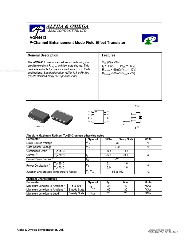
- G DFN 3x2
- S G S
The AON4413 uses advanced trench technology to provide excellent RDS(ON) with low gate charge. This device is suitable for use as a load switch or in PWM applications.