ASM3P2969A
ASM3P2969A is Low Power Peak EMI Reducing Solution manufactured by Alliance Semiconductor Corporation.
September 2005
.. rev 1.6
Low Power Peak EMI Reducing Solution
Features
- -
- -
- -
- - Generates an EMI optimized clock signal at the output. Integrated loop filter ponents. Operates with a 3.3V / 2.5V supply. Operating current less than 4m A. Low power CMOS design. Input frequency range: 6MHz to 12MHz for 2.5V : 6MHz to 13MHz for 3.3V Generates a 1X low EMI spread spectrum clock of the input frequency. Frequency deviation: ±1% @ 10MHz Available in 6 pin TSOT-23, 8 pin SOIC and 8 pin TSSOP Packages.
The ASM3P2969A uses the most efficient and optimized modulation profile approved by the FCC and is implemented by using a proprietary all digital method. The ASM3P2969A modulates the output of a single PLL in order to “spread” the bandwidth of a synthesized clock, and more importantly, decreases the peak amplitudes of its harmonics. This results in significantly lower system EMI pared to the typical narrow band signal produced by oscillators and most frequency generators. Lowering EMI by increasing a signal’s bandwidth is called ‘spread spectrum clock generation’.
- Applications
The ASM3P2969A is targeted towards all portable devices with very low power requirements like MP3 players, Notebooks and digital still cameras.
Product Description
The ASM3P2969A is a versatile spread spectrum frequency modulator designed specifically for a wide range of clock frequencies. The ASM3P2969A reduces electromagnetic interference (EMI) at the clock source, allowing system wide reduction of EMI of all clock dependent signals. The ASM3P2969A allows significant system cost savings by reducing the number of circuit board layers ferrite beads, shielding that are traditionally required to pass EMI regulations.
Key Specifications Description
Supply voltages Cycle-to-Cycle Jitter Output Duty Cycle Modulation Rate Equation Frequency Deviation
Specification
VDD = 3.3V /2.5V 200p S (Max) 45/55% FIN/256 ±1% @ 10MHz
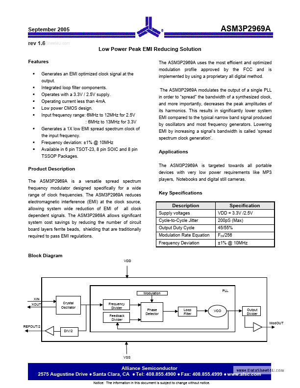
Block Diagram
Modulation XIN XOUT...