UT9Q512K32E Overview
Description
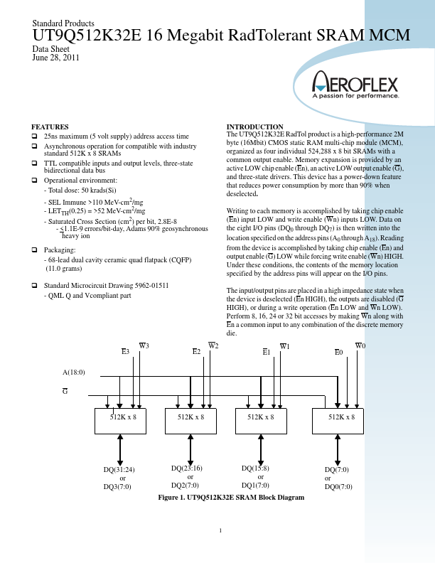
The UT9Q512K32E RadTol product is a high-performance 2M byte (16Mbit) CMOS static RAM multi-chip module (MCM), organized as four individual 524,288 x 8 bit SRAMs with a common output enable. Memory expansion is provided by an active LOW chip enable (En), an active LOW output enable (G), and three-state drivers.
Key Features
- Total dose: 50 krads(Si)
- SEL Immune >110 MeV-cm2/mg
- LETTH(0.25) = >52 MeV-cm2/mg
- Saturated Cross Section (cm2) per bit, 2.8E-8
- <1.1E-9 errors/bit-day, Adams 90% geosynchronous heavy ion Packaging