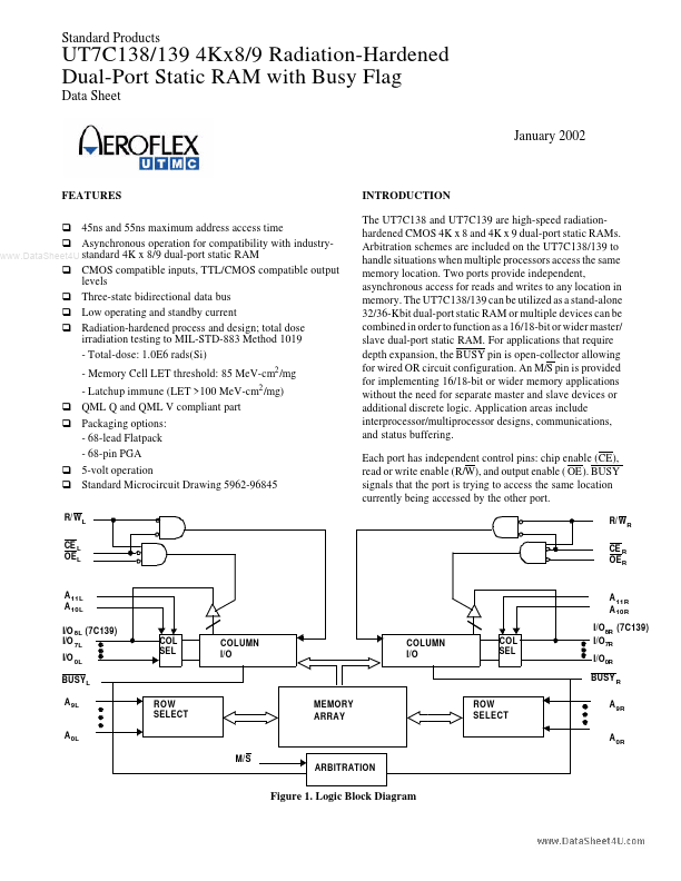
Description
3
The UT7C138/139 consists of an array of 4K words of 8 or 9 bits of dual-port SRAM cells, I/O and address lines, and control signals (CE, OE, R/W).These control pins permit independent access for reads or writes to any location in memory.To handle simultaneous writes/reads to the same location, a BUSY pin is provided on each port.With the M/S pin, the UT7C138/139 can function as a master (BUSY pins are outputs) or as a slave (BUSY pins are inputs).Each port is provided with its own output
Features
- q 45ns and 55ns maximum address access time q Asynchronous operation for compatibility with industrystandard 4K x 8/9 dual-port static RAM www. DataSheet4U. com q CMOS compatible inputs, TTL/CMOS compatible output levels q Three-state bidirectional data bus q Low operating and standby current q Radiation-hardened process and design; total dose irradiation testing to MIL-STD-883 Method 1019 - Total-dose: 1.0E6 rads(Si) - Memory Cell LET threshold: 85 MeV-cm2 /mg q q - Latchup immune (LET >100 MeV-c.