AP9924GO
AP9924GO is N-CHANNEL ENHANCEMENT MODE POWER MOSFET manufactured by Advanced Power Electronics Corp.
Description
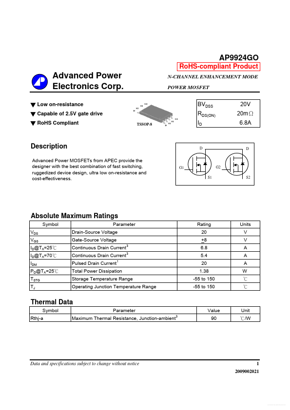
Advanced Power MOSFETs from APEC provide the designer with the best bination of fast switching, ruggedized device design, ultra low on-resistance and cost-effectiveness.
G1 S1
G2 S2
Absolute Maximum Ratings
Symbol VDS VGS ID@TA=25℃ ID@TA=70℃ IDM PD@TA=25℃ TSTG TJ Parameter Drain-Source Voltage Gate-Source Voltage Continuous Drain Current Continuous Drain Current Pulsed Drain Current
1 3 3
Rating 20 +8 6.8 5.4 20 1.38 -55 to 150 -55 to 150
Units V V A A A W ℃ ℃
Total Power Dissipation Storage Temperature Range Operating Junction Temperature Range
Thermal Data
Symbol Rthj-a Parameter Maximum Thermal Resistance, Junction-ambient
Value 90
Unit ℃/W
Data and specifications subject to change without notice
1 2009002021
Free Datasheet http://../
Electrical Characteristics@Tj=25o C(unless otherwise specified)
Symbol BVDSS RDS(ON) Parameter Drain-Source Breakdown Voltage Static Drain-Source On-Resistance
Test Conditions VGS=0V, ID=250u A VGS=4.5V, ID=6A VGS=2.5V, ID=4A
Min. 20 0.25
- Typ. 19 9 1 4.5 8 10 16 7 400 120 110
Max. Units 20 30 1 10 +100 14.4 640 V mΩ mΩ V S u A n A n C n C n C ns ns ns ns p F p F p F
VGS(th) gfs IDSS IGSS Qg Qgs Qgd td(on) tr td(off) tf Ciss Coss Crss
Gate Threshold Voltage Forward Transconductance Drain-Source Leakage Current Gate-Source Leakage Total Gate Charge
VDS=VGS, ID=250u A VDS=10V, ID=6A VDS=20V, VGS=0V VGS= +8V, VDS=0V ID=6A VDS=16V VGS=4.5V VDS=10V ID=1A RG=3.3Ω,VGS=5V RD=10Ω VGS=0V VDS=20V f=1.0MHz
Gate-Source Charge Gate-Drain ("Miller") Charge Turn-on Delay Time Rise Time Turn-off Delay Time Fall Time Input Capacitance Output Capacitance Reverse Transfer Capacitance
Source-Drain Diode
Symbol VSD trr Qrr Parameter Forward On Voltage
2 2
Test Conditions IS=1.2A, VGS=0V IS=6A, VGS=0V, d I/dt=100A/µs
Min.
- Typ. 24 15
Max. Units 1.2 V ns n...