AP04N60H-H-HF
AP04N60H-H-HF is N-CHANNEL ENHANCEMENT MODE POWER MOSFET manufactured by Advanced Power Electronics Corp.
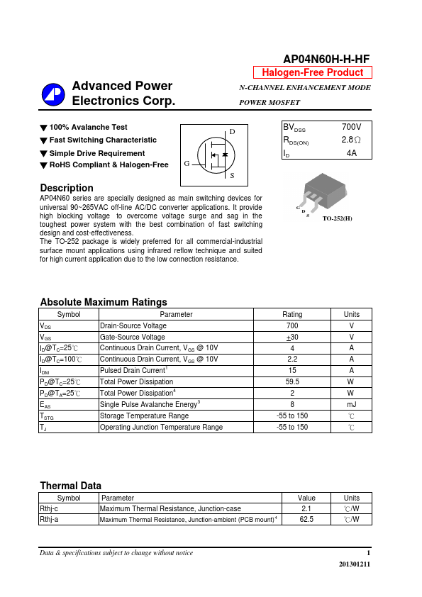
Description
AP04N60 series are specially designed as main switching devices for universal 90~265VAC off-line AC/DC converter applications. It provide high blocking voltage to overe voltage surge and sag in the toughest power system with the best bination of fast switching design and cost-effectiveness. The TO-252 package is widely preferred for all mercial-industrial surface mount applications using infrared reflow technique and suited for high current application due to the low connection resistance.
TO-252(H)
Absolute Maximum Ratings http://..net/
Symbol VDS VGS ID@TC=25℃ ID@TC=100℃ IDM PD@TC=25℃ PD@TA=25℃ EAS TSTG TJ
Parameter Drain-Source Voltage Gate-Source Voltage Continuous Drain Current, V GS @ 10V Continuous Drain Current, V GS @ 10V Pulsed Drain Current
Rating 700 +30 4 2.2 15 59.5
Units V V A A A W W m J ℃ ℃
Total Power Dissipation Total Power Dissipation
4 3
2 8 -55 to 150 -55 to 150
Single Pulse Avalanche Energy Storage Temperature Range
Operating Junction Temperature Range
Thermal Data
Symbol Rthj-c Rthj-a Parameter Maximum Thermal Resistance, Junction-case
Maximum Thermal Resistance, Junction-ambient (PCB mount)
Value 2.1 62.5
Units ℃/W ℃/W
Data & specifications subject to change without notice
1 201301211 datasheet pdf
- http://..net/
Electrical Characteristics@Tj=25 C(unless otherwise specified)
Symbol BVDSS RDS(ON) VGS(th) gfs IDSS IGSS Qg Qgs Qgd td(on) tr td(off) tf Ciss Coss Crss Parameter Drain-Source Breakdown Voltage Static Drain-Source On-Resistance Gate Threshold Voltage Forward Transconductance Drain-Source Leakage Current Gate-Source Leakage Total Gate Charge Gate-Source Charge Gate-Drain ("Miller") Charge Turn-on Delay Time Rise Time Turn-off Delay Time Fall Time Input Capacitance Output Capacitance Reverse Transfer Capacitance
2 o
Test Conditions VGS=0V, ID=250u A VGS=10V, ID=2A VDS=VGS, ID=250u A VDS=10V, ID=2A VDS=480V, VGS=0V VGS=+30V, VDS=0V ID=1A VDS=480V VGS=10V VDD=300V ID=2A RG=50Ω...