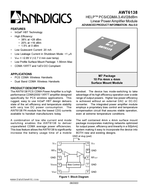
• Part: AWT6138
  • Description: LINEAR POWER AMPLIFIER
  • Manufacturer: ANADIGICS
  • Size: 241.69 KB
Download AWT6138 Datasheet PDF
ANADIGICS
AWT6138
AWT6138 is LINEAR POWER AMPLIFIER manufactured by ANADIGICS.
FEATURES • • High • • • In Ga P HBT Technology Efficiency: 38% at +28 d Bm 20% at +16 d Bm 1.5% at 0 d Bm • • • • • Low Quiescent Current: 20 m A Low Leakage Current in Shutdown Mode: <1 m A VREF = +2.85 V (+2.7 V min over temp) Low Profile Surface Mount Package: 1.56mm Max CDMA 1XRTT and 1x EV-DO pliant APPLICATIONS • • PCS CDMA Wireless Handsets Dual Band CDMA Wireless Handsets M7 Package 10 Pin 4mm x 4mm Surface Mount Module handset. The device has mode-switching to take advantage of its high efficiency operation over a wide range of output powers. Higher low power efficiency is achieved without an external DAC or DC-DC converter. The integrated power amplifier module employs a proprietary bias control and temperature pensation circuit that assures stable operation, even at extreme temperature conditions. The self contained 4mm x 4mm surface mount package incorporates matching networks optimized for output power, efficiency and linearity in a 50[ohm] system making it easy to incorporate the device into BOTH new and existing designs. GND at slug (pad) PRODUCT DESCRIPTION The AWT6138 PCS CDMA Power Amplifier is a high performance CDMA2000/ 1XRTT amplifier designed specifically for PCS wireless applications. This rugged, easy to use In Ga P HBT design delivers state of the art efficiency and temperature stability with very low DC power consumption. The AWT6138 PA module has the lowest CDG currents available to handset manufacturers today. A bination of low idle current and mode switching enables the AWT6138 to deliver unparalleled CDMA average power efficiencies. This bias feature allows the AWT6138 to significantly increase the battery usage time of a mobile VCC RFIN GND 1 2 3 Bias Control 10 VCC 9 8 7 6 GND RFOUT GND GND VMODE 4 VREF 5 Figure 1: Block Diagram 09/2003 GND VCC RFIN GND VMODE VREF 1 2 3 4 5 GND .. 10 VCC 9 8 7 6 GND RFOUT GND GND Figure 2: Pinout (X-ray Top View) Table 1: Pin Description PIN 1 2 3 4 5 6 7 8 9 10 NAME V CC RFIN GND...