Datasheet Summary
21&[
®
$0,+- PLFURQ &026
- DWH $UUD
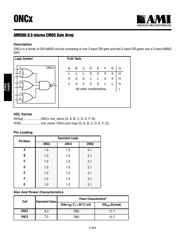
Description
ONCx is a family of OR-NAND circuits consisting of one 3-input OR gate and two 2-input OR gates into a 3-input NAND gate.
Logic Symbol
Truth Table
ONCx
A BCDE FGQ
B L L LXXXXH
XXXL LXXH
Q XXXXXL LH
All other binations
Core Logic
HDL Syntax Verilog .................... ONCx inst_name (Q, A, B, C, D, E, F, G); VHDL...................... inst_name: ONCx port map (Q, A, B, C, D, E, F, G);
Pin Loading
Pin Name
A B C D E F G
ONC2 1.0 1.0 1.0 1.0 1.0 1.0 1.0
Equivalent Loads ONC4 1.0 1.0 1.0 1.0 1.0 1.0 1.0
ONC6 2.1 2.1 2.1 2.1 2.1 2.1 2.1
Size And Power Characteristics
Power Characteristicsa
Cell...