The following content is an automatically extracted verbatim text
from the original manufacturer datasheet and is provided for reference purposes only.
View original datasheet text
21�[
®
$0,�+* ��� PLFURQ &026 *DWH $UUD
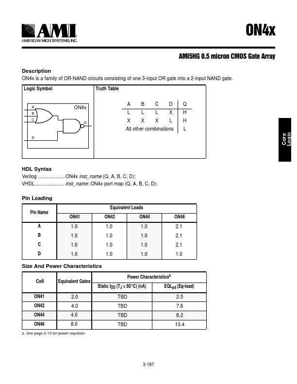
Description ON4x is a family of OR-NAND circuits consisting of one 3-input OR gate into a 2-input NAND gate.
Logic Symbol
Truth Table
A ON4x A B C D Q B L L LXH C Q XXXLH
All other combinations L
D
Core Logic
HDL Syntax Verilog .................... ON4x inst_name (Q, A, B, C, D); VHDL...................... inst_name: ON4x port map (Q, A, B, C, D);
Pin Loading
Pin Name
A B C D
ON41 1.0 1.0 1.0 1.0
Equivalent Loads
ON42
ON44
1.0 1.0
1.0 1.0
1.0 1.0
1.0 1.0
ON46 2.1 2.1 2.1 1.0
Size And Power Characteristics
Power Characteristicsa
Cell Equivalent Gates
Static IDD (TJ = 85°C) (nA)
EQLpd (Eq-load)
ON41
2.0
TBD
2.5
ON42
4.0
TBD
7.6
ON44
4.0
TBD
8.2
ON46
8.0
TBD
13.4
a. See page 2-15 for power equation.
 ON42 Datasheet