Datasheet Details
| Part number | ODTSXN04 |
|---|---|
| Manufacturer | AMI |
| File Size | 25.34 KB |
| Description | CMOS Gate Array |
| Datasheet |
 ODTSXN04 Datasheet ODTSXN04 Datasheet
|
|
|
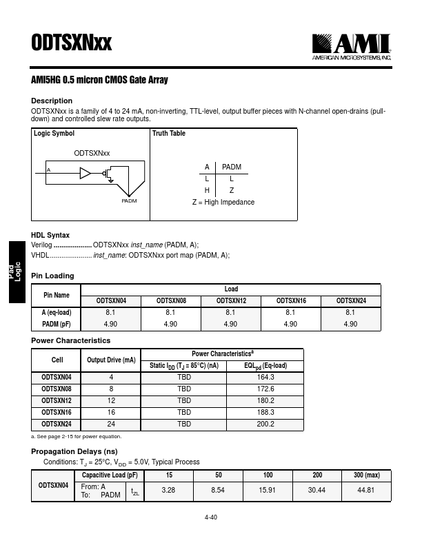
ODTSXNxx is a family of 4 to 24 mA, non-inverting, TTL-level, output buffer pieces with N-channel open-drains (pulldown) and controlled slew rate outputs.
| Part number | ODTSXN04 |
|---|---|
| Manufacturer | AMI |
| File Size | 25.34 KB |
| Description | CMOS Gate Array |
| Datasheet |
ODTSXN04 Datasheet
|
|
|
|
| Part Number | Description | Manufacturer |
|---|
| Part Number | Description |
|---|---|
| ODTSXN08 | CMOS Gate Array |
| ODTSXN12 | CMOS Gate Array |
| ODTSXN16 | CMOS Gate Array |
| ODTSXN24 | CMOS Gate Array |
| ODTSXE04 | CMOS Gate Array |
The following content is an automatically extracted verbatim text from the original manufacturer datasheet and is provided for reference purposes only.