ODCXXE04 Overview
Description
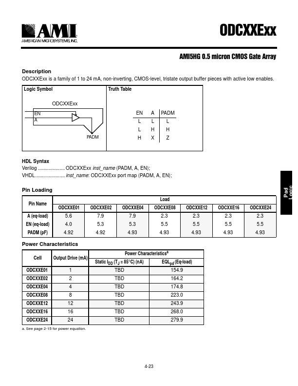
ODCXXExx is a family of 1 to 24 mA, non-inverting, CMOS-level, tristate output buffer pieces with active low enables. Logic Symbol Truth Table ODCXXExx EN A PADM EN A PADM LL L LH H HX Z HDL Syntax Verilog.
| Part | ODCXXE04 |
|---|---|
| Description | CMOS Gate Array |
| Manufacturer | AMI |
| Size | 31.58 KB |
ODCXXExx is a family of 1 to 24 mA, non-inverting, CMOS-level, tristate output buffer pieces with active low enables. Logic Symbol Truth Table ODCXXExx EN A PADM EN A PADM LL L LH H HX Z HDL Syntax Verilog.
| Part Number | Manufacturer | Description |
|---|---|---|
| CTA2P1N | Diodes Incorporated | COMPLEX TRANSISTOR ARRAY |
| CTA2N1P | Diodes Incorporated | COMPLEX TRANSISTOR ARRAY |
| 7003 | Allegro MicroSystems | HIGH-VOLTAGE/ HIGH-CURRENT DARLINGTON ARRAY |