Datasheet Details
| Part number | ODCSXX04 |
|---|---|
| Manufacturer | AMI |
| File Size | 23.70 KB |
| Description | CMOS Gate Array |
| Datasheet |
 ODCSXX04 Datasheet ODCSXX04 Datasheet
|
|
|
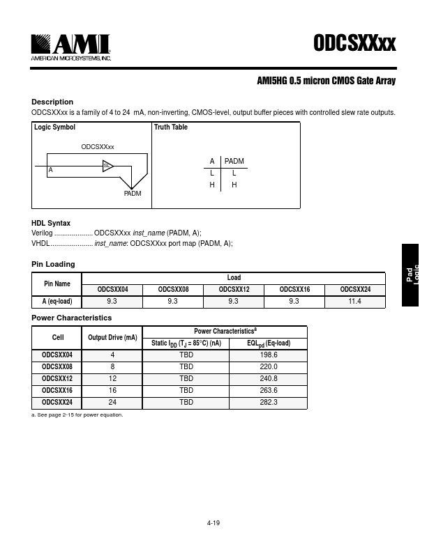
ODCSXXxx is a family of 4 to 24 mA, non-inverting, CMOS-level, output buffer pieces with controlled slew rate outputs.
| Part number | ODCSXX04 |
|---|---|
| Manufacturer | AMI |
| File Size | 23.70 KB |
| Description | CMOS Gate Array |
| Datasheet |
ODCSXX04 Datasheet
|
|
|
|
| Part Number | Description | Manufacturer |
|---|---|---|
| ODC24 | I/O Module | Crydom |
| ODC24A | I/O Module | Crydom |
| ODC24F | I/O Module | Crydom |
| ODC5 | I/O Module | Crydom |
| ODC5A | I/O Module | Crydom |
| Part Number | Description |
|---|---|
| ODCSXX08 | CMOS Gate Array |
| ODCSXX12 | CMOS Gate Array |
| ODCSXX16 | CMOS Gate Array |
| ODCSXX24 | CMOS Gate Array |
| ODCSXE04 | CMOS Gate Array |
The following content is an automatically extracted verbatim text from the original manufacturer datasheet and is provided for reference purposes only.