Download the S-5743NBL1A datasheet PDF.
This datasheet also covers the S-5743xxA variant, as both devices belong to the same bipolar hall-effect latch family and are provided as variant models within a single manufacturer datasheet.
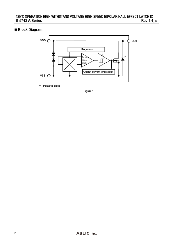
Description
GND pin Power supply pin Output pin
Figure 2
Absolute Maximum Ratings
Table 4
(Ta = +25°C unless otherwise specified)
Item
Symbol
Absolute Maximum Rating
Unit
Power supply voltage Output current Output voltage Operation ambient temperature
VDD IOUT VOUT Topr
VSS
0.3 to VSS
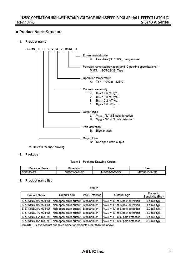
Features
- Pole detection:.
- Output logic.
- 1:.
- Output form:.
- Magnetic sensitivity.
- 1:.
- Chopping frequency:.
- Output delay time:.
- Power supply voltage range:.
- Built-in regulator.
- Built-in output current limit circuit.
- Operation temperature range:.
- Lead-free (Sn 100%), halogen-free.
- 1. The option can be selected. Bipolar latch VOUT = "L" at S pole detection VOUT = "H" at S pole detection Nch open-drai.
 S-5743NBL1A Datasheet