GS81302T37GE Key Features
- 2.0 Clock Latency
- Simultaneous Read and Write SigmaDDR™ Interface
- mon I/O bus
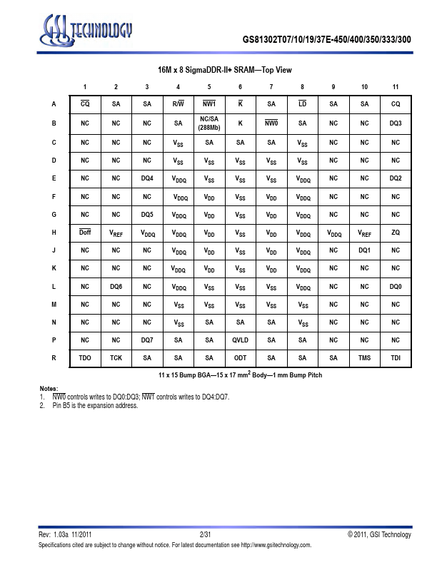
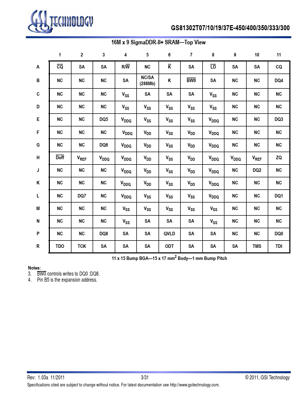
- JEDEC-standard pinout and package
- Double Data Rate interface
- Byte Write controls sampled at data-in time
- Burst of 2 Read and Write
- On-Die Termination (ODT) on Data (D), Byte Write (BW)
- 1.8 V +100/-100 mV core power supply
- 1.5 V or 1.8 V HSTL Interface